He Tingbo says her epiphany came from an ancient irrigation system in Sichuan province, built without modern machinery or electricity
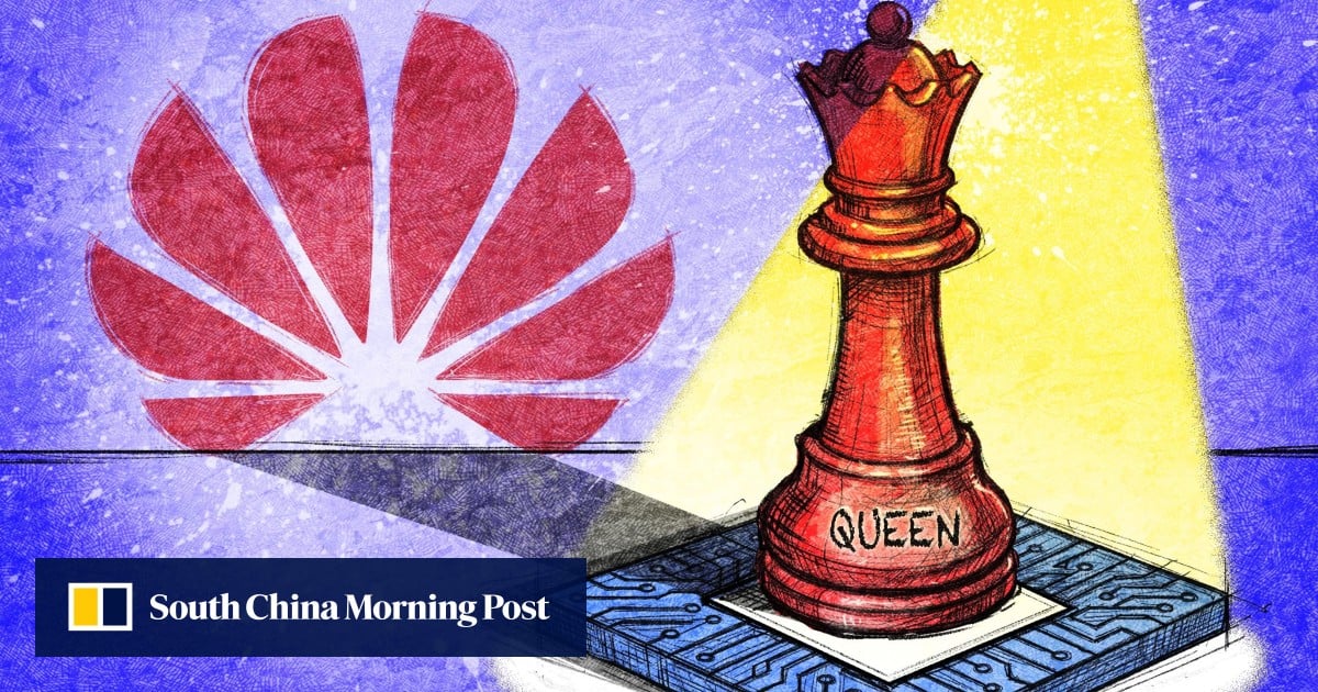
6-MIN READ6-MINAnn Caoin ShanghaiandIris Dengin ShenzhenPublished: 10:00am, 13 Jun 2026After seven years working in the shadows, He Tingbo stepped back into the limelight last month.The head of Huawei Technologies’ secretive semiconductor business – widely dubbed the company’s “chip queen” – had been out of the public view since 2019, when Washington severed the Chinese company’s global access to advanced technology, including semiconductors.
Her retreat into the background became a symbol of Huawei’s battle for survival. That all changed last month on a global academic stage in Shanghai – the IEEE International Symposium on Circuits and Systems.
It was there that He introduced the “Tau (τ) Scaling Law”, which Huawei claimed could achieve transistor densities equivalent to the cutting-edge 1.4-nanometre process by 2031 – all without the need for advanced extreme ultraviolet (EUV) lithography machines out of reach due to US sanctions.
For half a century, the electronics industry treated Moore’s Law – the principle that the number of transistors on a chip doubles roughly every two years – as gospel. But as silicon structures approached atomic limits, geometric scaling was yielding diminishing economic returns and hitting an architectural brick wall.